Important: Hi! If you want to receive a notification when the system is ready-to-deploy, consider checking out the Pulsar’s website here where you’ll be able to subcribe to the newsletter (we’ll only send out emails for the launch day, no spam).
Note: Checkout this blog for regular updates regarding the prototype assembly and testing and the software development.
Warning: Attention! This project is currently under rapid development so some of the content below might not be available yet or incorrect.
Caution: Always check with local authority about RF bands regulations in your area.
This document contains an overview of the project, a simple description of its parts and its development process, basic instructions on how to build your own Pulsar and how to use it, along with some renders and pictures.
I hope you will enjoy the process and you are always welcome to open an issue for feedbacks and questions.
- Want to know more about the project? Take a look at the synopsis.
- Curious about the development? Read more here.
- Interested in the software behind the Pulsar? This way.
- Ready to build your own Pulsar? Jump here.
Synopsis
The Pulsar is a highly portable, off-grid (and optionally on-grid), modular radio communication system. The goal is to create a small (hand-held), battery powered, system that can operate on multiple radio frequencies and use high-power RF power amplifiers to allow long-range, decentralized, reliable and secure, communication between two or more nodes.
The modular design allows swapping of the RF modules independently of the main computer (CLU), keeping one standard interface for unlimited customizable setups.
Through the use of an optional 4G/5G module, the system can also communicate via traditional networks. Due to the need of a SIM to authenticate the user on a commercial network, this module, if installed, can be shutdown at any moment by the uC by removing all power to the module. To operate the 4G/5G module an SBC running OpenWRT is needed. This way the main computer will have access to the 4G/5G lines through serial connetion to the SBC and you will have a fully featured router and 4G/5G modem that you can directly connect to via a dedicated wifi AP.
Working Principle: The main computer (CLU) can connect to other devices (like smartphones, computers and even CSRF controllers) via bluetooth LE and serial wired ports. The conneted devices can send, via the serial line with the main computer, data that they need to send over the radio link. The main computer then uses the RF modules to communicate with another Pulsar (or compatible device), and send the data (encrypted). Once it’s on the other Pulsar it can be sent via serial connection to the specific destination device that is connected to it.
Licensing
The system is open-source and open-hardware so that anybody that is interested can build one on its own and even modify the design or give his/her feedback.
The hardware is released under the CERN-OHL-S license (In particular, everything under 3D Files and PCB Files), while all software is released under GNU-Affero-GPL-V3 license.
Table of contents
Important: To keep this guide simple and understandable, in the following chapters I will refer to a particular configuration of the modules and parts, although the user knows that the system is highly customizable and can be changed from start to finish. The configuration that I will refer to is as follows: 3S battery, DCDC with 5.0V@3A, 3.3V@2A and 3.8V@3A (for the LTE modem), a Raspberry Pi 3B SBC or similar WiFi and USB3 capable SBC, a Quectel LTE EM05 modem, a generic UART GNSS 5V module, a single SX1281 2.4 GHz module powered from the 3.3 V and a single SX1262 868 MHz module powered from the 5.0 V.
Sponsors

A special thank you to PCBWay for reaching out and offering to help with the development of the project. Without their help I would not be working on a new PCB iteration with improved design and better capability. For this project I am going to rely on their PCB production and assembly services, but they offer many other great services like PCB design, CNC machining and 3D printing. If you are working on a DIY project of any sort I suggest you check them out here.
Repository Structure
The repository is divided into 3 sections.
- The base folder along with the Images folder contains the README, LICENSE and some useful informations to get started. All of the informations contained in these folders are accessible in an organized matter in this README.
- The 3D Files folder contains 3D files (mainly STEP) that you will need to print to build your Pulsar (read more about this here). It also contains some 3D models of the PCBs so that you can use them if you wish to integrate the PCBs into your own design.
- The PCB Files folder contains gerber files to send to your preferred PCB manufacturer, BOM files so that you can order all necessary components and the PCB’s schematics.
Technical Overview
Over this chapter I’m going to talk about each of the parts that make up the system, from the electronics to the 3D printed case.
To give a general overview of the project, I’ll give a quick list of its parts. The Pulsar is powered by a battery (3S LiPo/LiIon), uses a DC/DC PSU to power the main logic board (CLU), the two LoRa RF modules, the Quectel modem, the router SBC and the GPS module. There’s also a rotary selector and a small display that the user can interface with. A 3D printed case encloses everything.
Central Logic Unit
The main board, or CLU, connects together all modules and user interfaces. It does not provide power, that is left to the PSU.
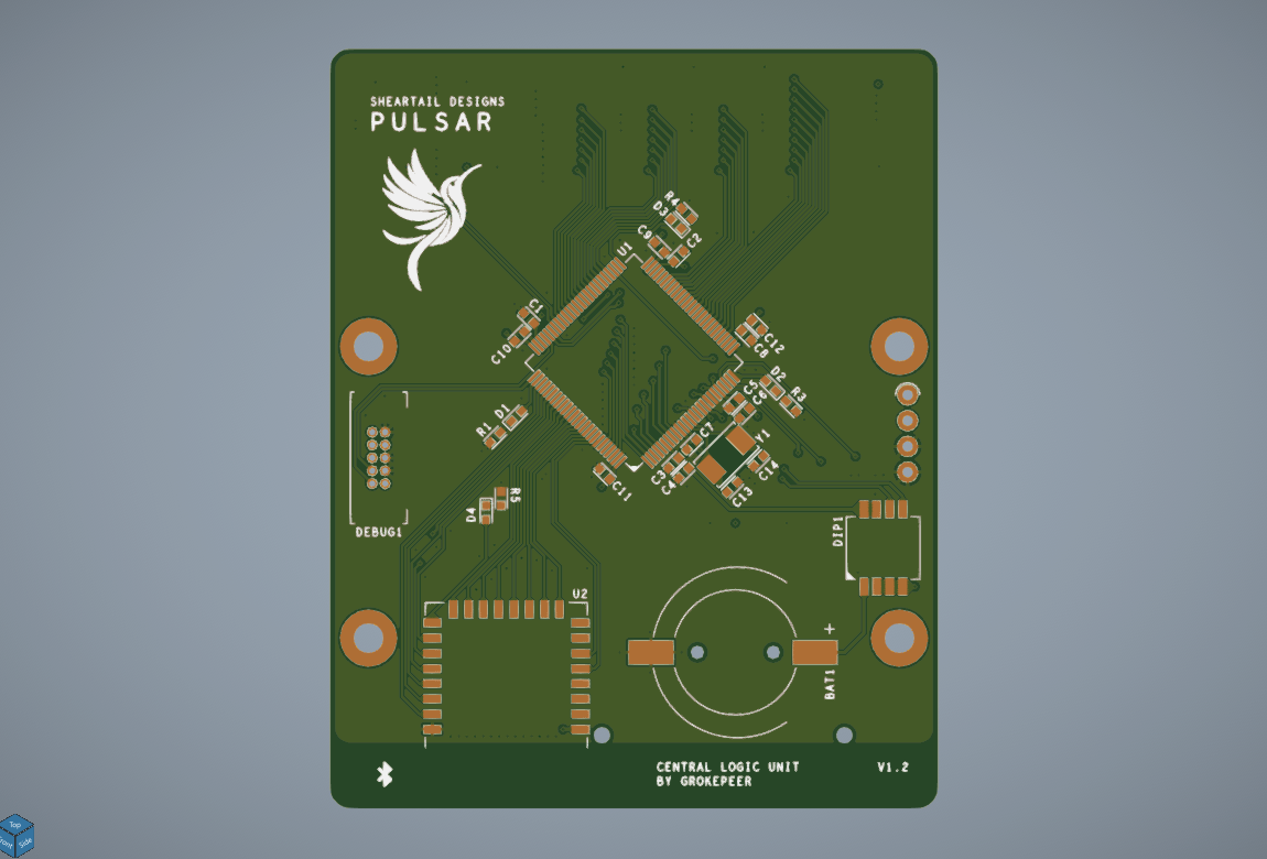
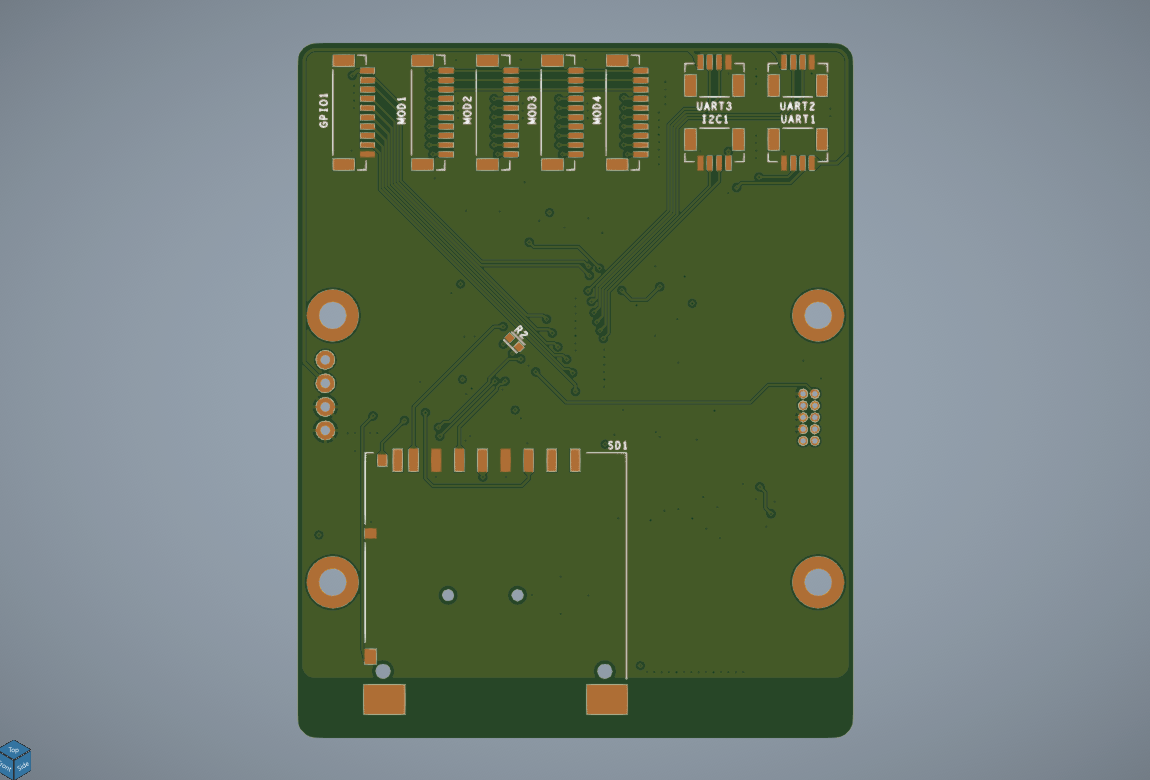
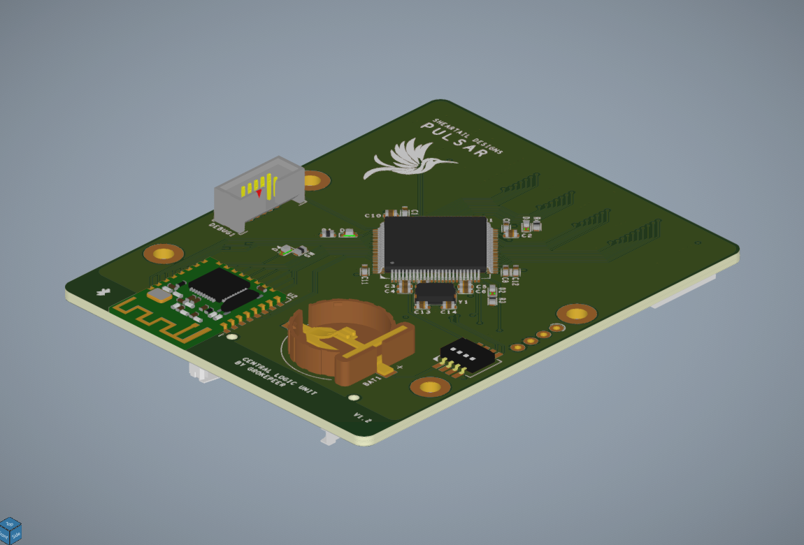
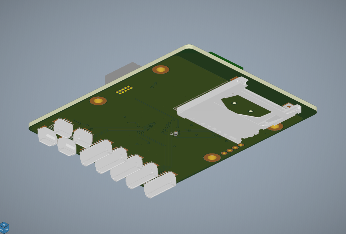
The board has 4 MODx connectors that offer multiple GPIOs and an SPI interface, to connect to the RF modules (in particular, to connect directly to the SemTech SX1262 and SX1281 chips), 3 UARTs, one used to connect to the SBC, one for the GPS module and the third is left to allow external computers or controllers to connect, a single I2C that is used to connect to a small screen and a GPIO header that connects to various user interfaces.
On the baord you will also find an SD card slot that allows the system to save log files during operation, a coin battery that allows the internal RTC to remain active without the main battery, a small DIP switch that is used for configuration of the board, the JDY-23 bluetooth module, and the STM32H733VGT6 at the heart of the system with its debug interface connector (SWD).
The CLU inside the Pulsar is a simple 4 layer, 60 x 75 mm PCB, that can be hand-soldered.
Power Supply Unit
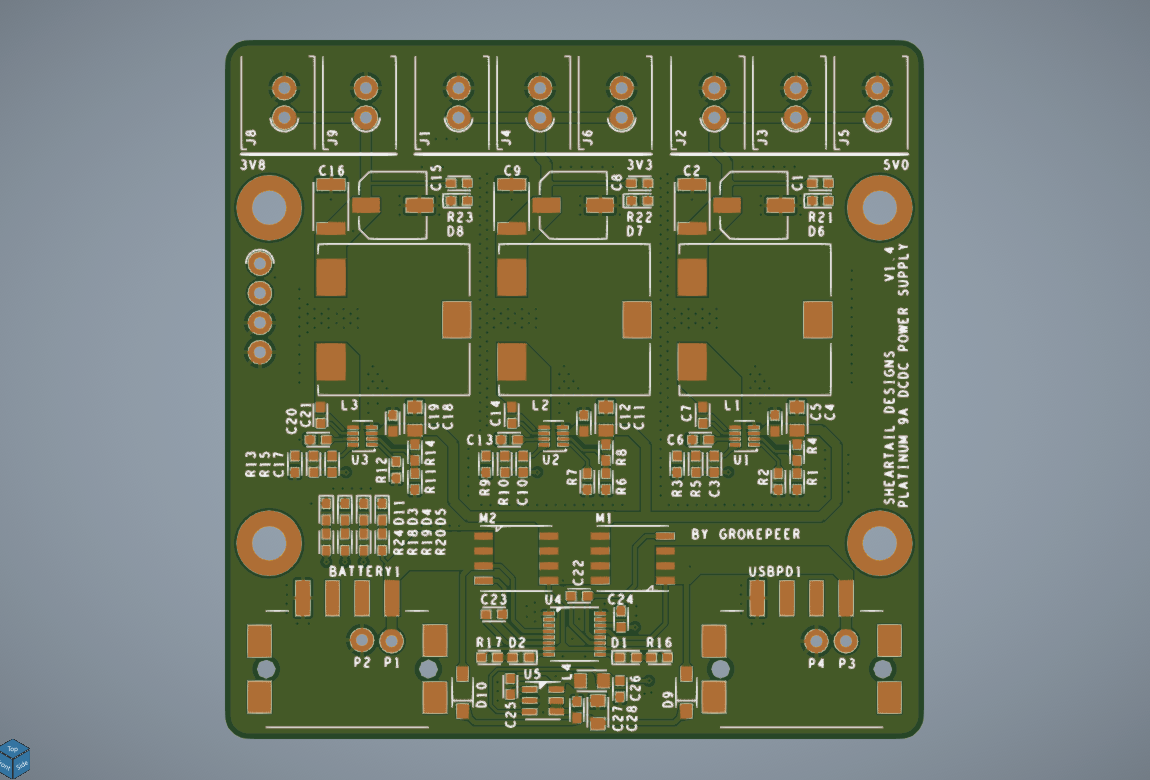
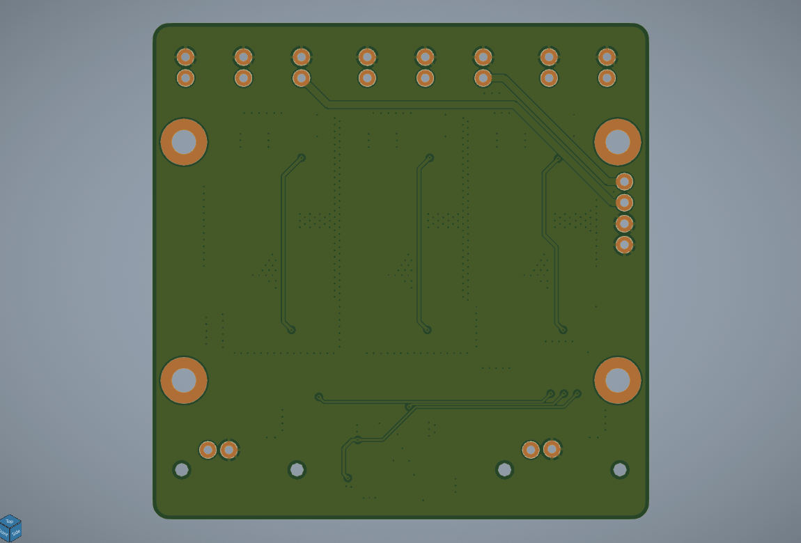
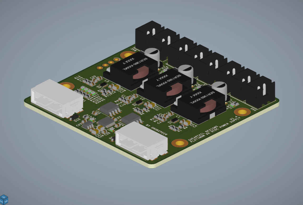
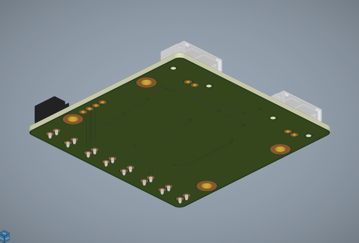
To power the entire system with high-power RF modules, microcontrollers, an SBC and a 4G/5G modem, a proper DC/DC power supply is necessary. The RF modules use both 3.3 V and 5.0 V, the microcontroller uses 3.3V, the SBC uses 5.0 V and the Quectel modem uses 3.8 V, so it was necessary to design a 3 rail DC/DC PSU. To allow the addition of a more powerful RF PA further down the line the 3.8 V line can be reconfigured to a range of voltages using the feedback voltage divider in DCDC switching IC (check the board schematics for more details).
Each rail’s switching controller can be chosen between a 3 A variant and a 2 A one, depending on projected consumption. On my design I decided to go with two 3 A rails (3.8 V and 5.0 V) and a 2 A rail (3.3 V). Based on simulations the 3.3 V rail, powered at 15 V can reach 94.8% efficiency at 2A load. An ideal diode controller that can hot-swap between two power sources at voltages ranging from 8 V to 16 V is also integrated in the design.
The PSU inside the Pulsar is a 4 layer, 60 x 60 mm PCB, that can be hand-soldered.
Radio Modules
Since the modules are connected via the standard MODx connector you can integrate whatever radio module you want, as long as it can interface with the H733 using SPI. Software-wise I am planning to develop the firmware around “installable interface packages” that allow the user to add/remove interface packages based on connected modules, retaining legacy support while allowing maximum flexibility for the development of new modules. (I will explain this further when the system is developed)
The radio modules I decided to use are SemTech SX1262 and SX1281 based, and use LoRa modulation over a range of frequency as low as 100 MHz and as high as 2.4 GHz. LoRa is a popular, efficient and well adopted modulation system, so choosing it, rather then another, allows me to have access to a great choice of transceiver chips and plenty of documentation.
The specific modules I chose are from Ebyte: E22-xxxMxxS and E28-2G4MxxSX modules variaties. I then designed a simple carrier board that allows to connect both types of modules to the 10 pin MODx data connector and the power connector. It’s noteworthy that these LoRa modules, unlike others, even from the same Ebyte, expose direct communication to the SemTech chip, so the SPI interface is exactly the same I would have using different SX1262/SX1281 modules (even completely custom ones).
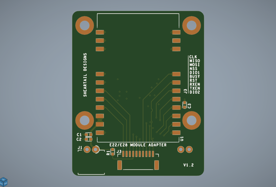
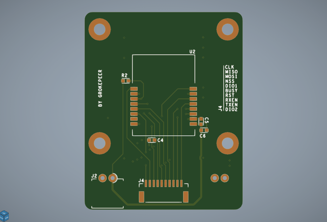
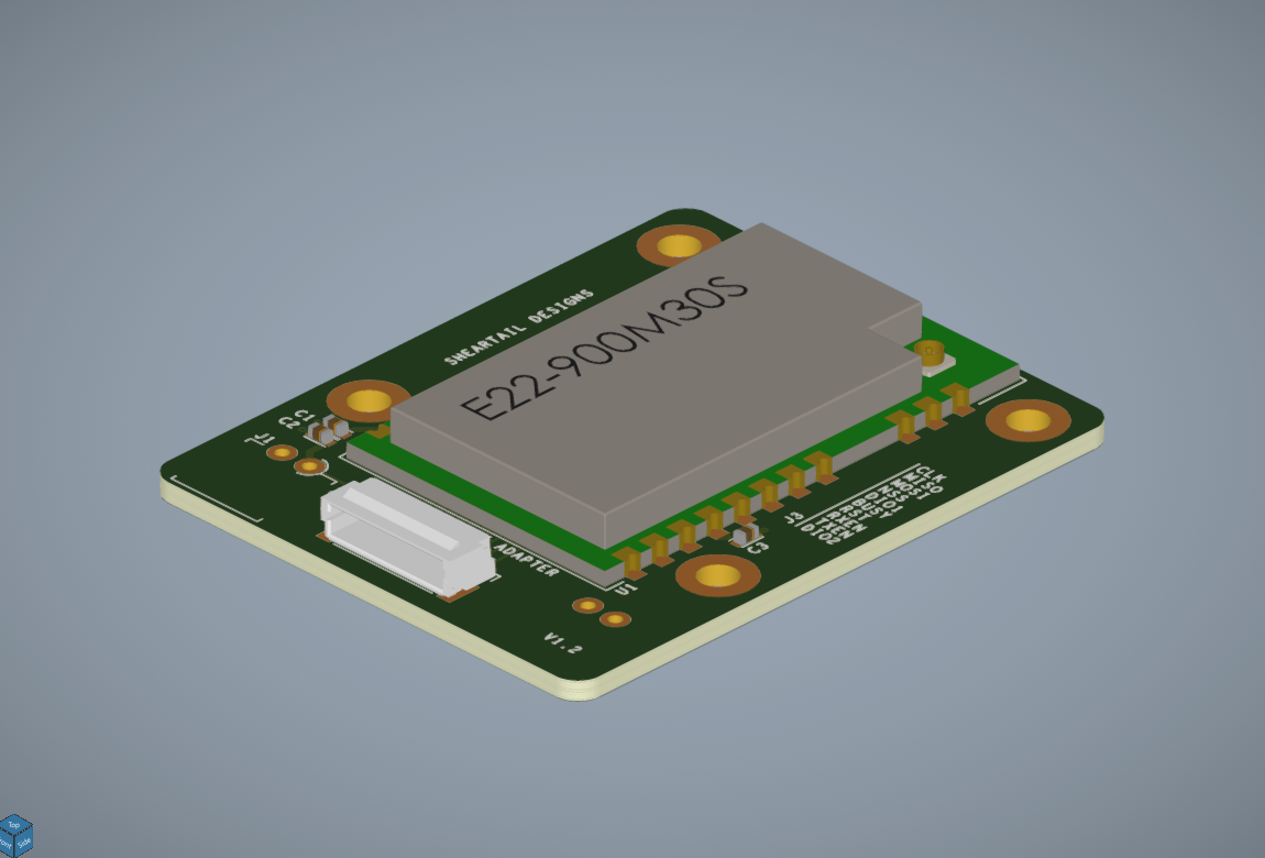
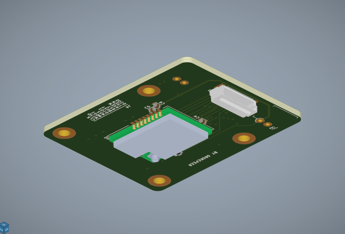
Router Module
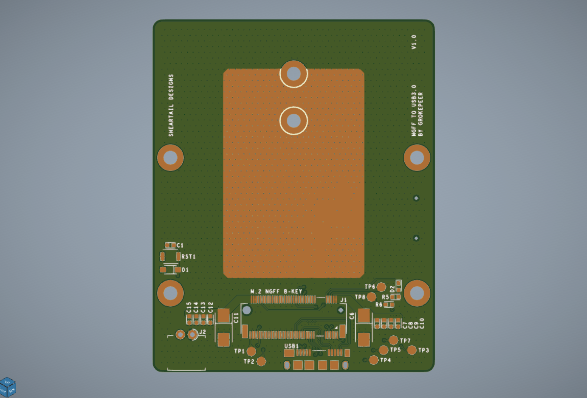
The “on-grid” module is composed of an SBC that operates as a normal router and an LTE module that is connected to the SBC via USB (using a NGFF M.2 to USB adapter). Any device that connects to the router can gain access to the on-grid line and can therefore navigate the web, etc.. Most 4G/5G modems integrate a GNSS chip and antenna that is disabled by default on this design because of privacy concerns.
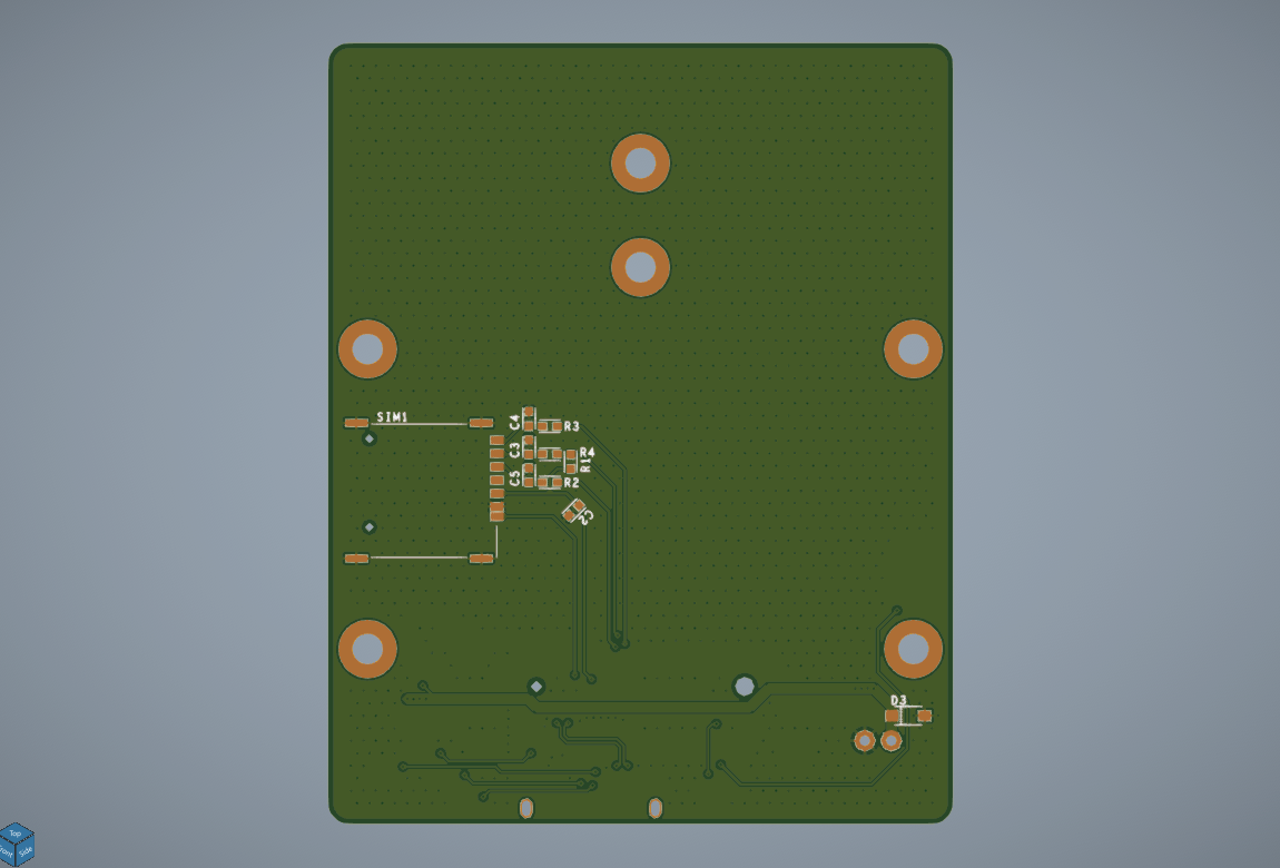
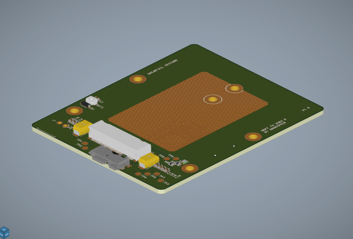
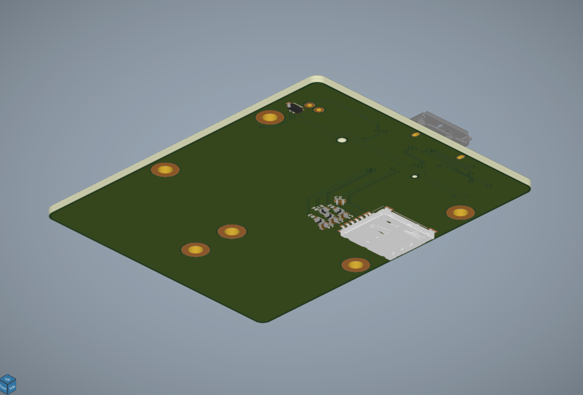
The SBC that I chose is the Raspberry Pi 3 Model B+ that I had laying around, but you can use more powerful, more up to date models with similar form factor. To connect a NGFF M.2 LTE module I then designed an adapter to USB. The adapter is a separate “entity” from the SBC so that based on availability and design needs, the SBC can be changed, while keeping the USB 4G/5G module intact. For this reason I won’t go into much detail about the SBC.
Because some CAT12+ LTE-A modems and 5G modems can saturate a single USB2.0 (480 Mbps) serial line, the board is designed with USB3.0 support (5.0 Gbps), requiring the design to incorporate impedance and phase matched lines.
Since some advanced modems consume a lot of power and produce plenty of heat, the board requires direct power from the DCDC (cannot be powered from USB at all) and presents a big heat-absorbing surface on the top side of the PCB, it also has copper pours on all layers and via arrays to help spread the heat from the modem.
The NGFF to USB3.0 adapter is a 4 layer, 60 x 75 mm PCB, that should be produced with a calculated stackup (more on this in the PCB sourcing section). It can be hand-soldered but I would suggest to leave the assembly of the NGFF and USB connector to a P&P machine.
Future Modules
The possiblities are endless and my ideas are usually way too ambitious but some of the modules I’d like to develop in the future are:
- Custom RF power amplifiers for more powerful radio modules designed for UHF and VHF.
- Custom HF radio modules that can be used for over-the-horizon radio communication.
- Perhaps a simple non-transmitting SDR module.
Still, the best part of the Pulsar is that you will be able to design your own hardware and write your own module interface package to integrate in the firmware!
Firmware and Software
The Pulsar hardware operates around one central microcontroller. This microcontroller runs the PulsarOS firmware. To connect to the Pulsar via BLE using a smartphone, the PulsarLoom app can be used. Other implementations of software interfaces (through BLE or serial) are not available yet, but can be purpose built with relative ease by anyone.
All the code for all the software and firmware is open-source and available in two dedicated repositories: PulsarOS and PulsarLoom. In the PulsarOS repository you’ll also find other code necessary for the peripherals present on the Pulsar, such as the Nordic BLE chip.
The following sections are going to focus on the PulsarOS firmware for the STM32H733VG microcontroller.
Basic Structure
The PulsarOS firmwares is built on top of FreeRTOS. This allows tasks to be dynamically scheduled when needed, reduces CPU load and helps with keeping everything as organized as possible during runtime.
The main task is represented by the radioTask, this task loads settings, initializes the radio modules and orchestrates communications with them. When this task doesn’t run a multitude of other tasks can operate without distrupting the radio, such as checking the battery voltage or updating the on-board display.
Module Interface
In order to allow any custom module to connect to the system, the PulsarOS is designed with external “translation layers” that transform standard instructions from the PulsarOS to specific ones meant for the particular module that they refer to. This functionality is achieved using a standard interface between the “translation layer” and the PulsarOS core, that exposes to both a set of functions that both parts can call in order to command the other. To give an example, if the core needs to send a message via the module number 1, it’s going to load the module 1 interface (our “translation layer”) and call a certain “send(msg)” function. The interface will then have all the instructions necessary for the radio module to actually send the message. This way the core only needs to decide when to send what message, regardless of what modules are installed. Providing a strong compatibility with both future and legacy modules.
Debugging Tools
When working on this much code a good set of debugging tools is a great way to improve your productivity and possibly reduce wasted time.
As a programming and debugging probe I always use the ST-LINK V3 MINIE with the original firmware on it. But there are lots of different options out there depending on budget, needs and platform.
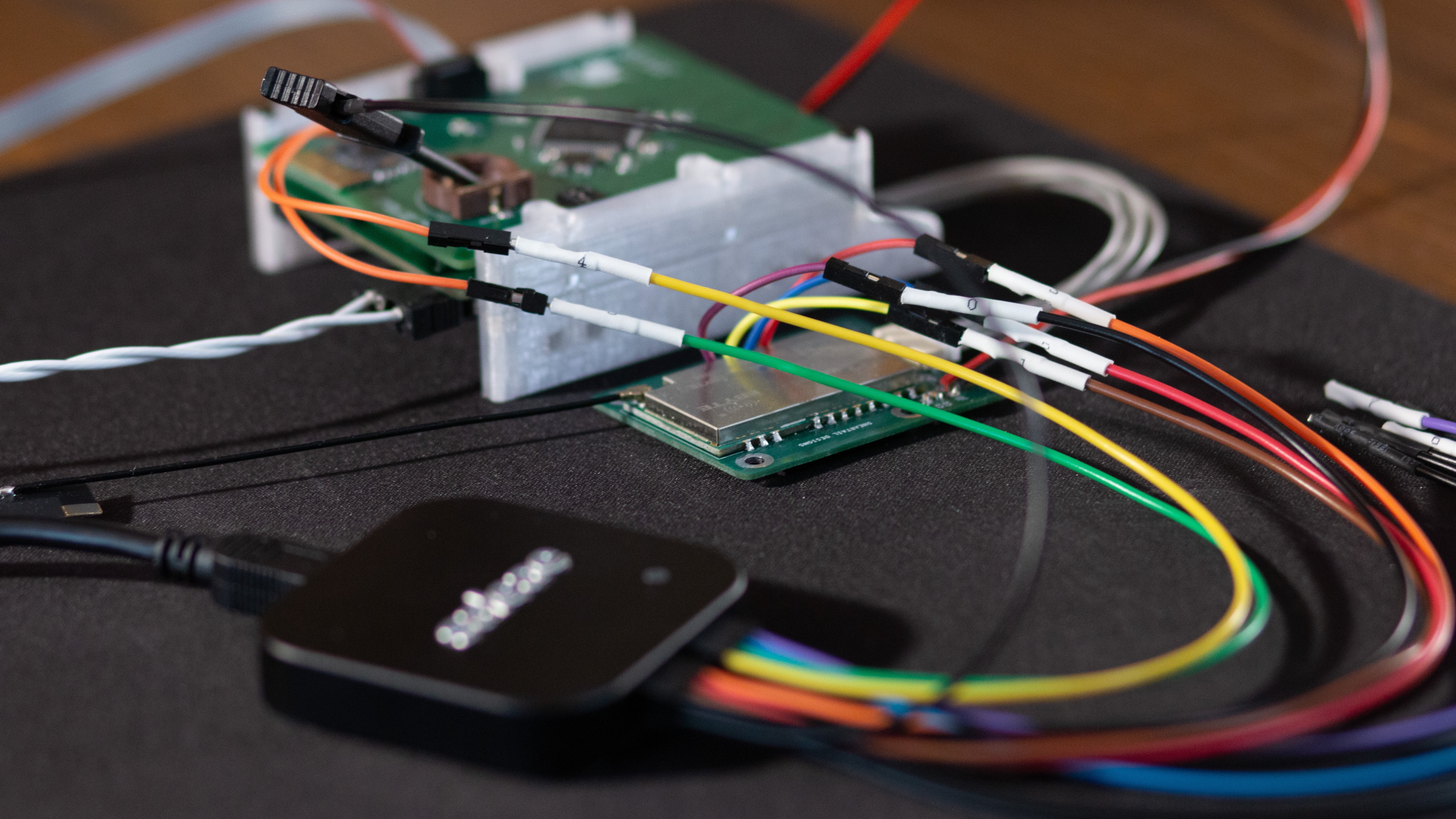
For the software development of the PulsarOS I also decided to get myself a logic analyzer. Since there’re so many peripherals to work with and so many different serial lines to operate I knew I was going to loose a lot of time chasing bugs if I didn’t get a logic analyzer. For this reason, after a lot of research, I bought the Saleae Logic 8.
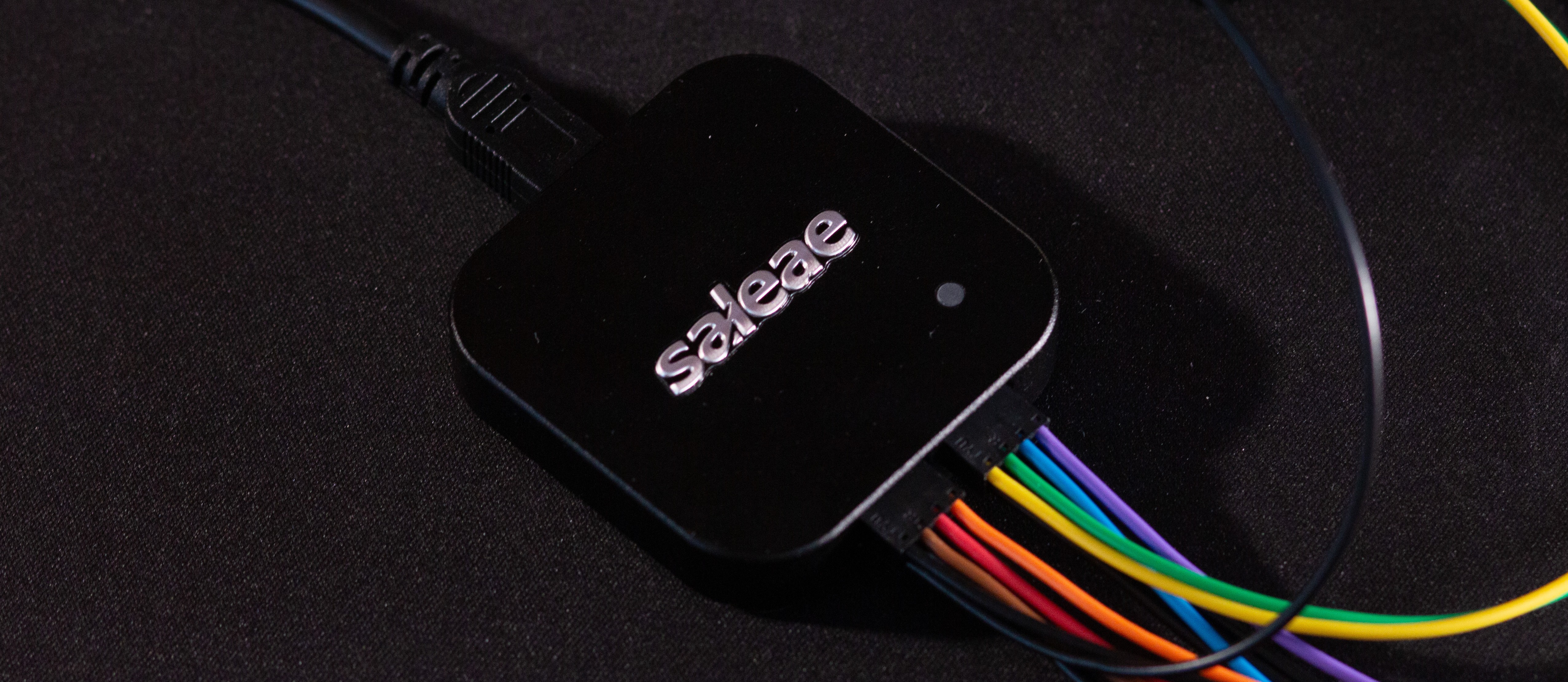
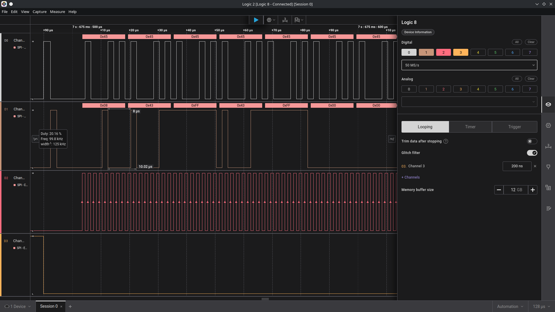
After just a bit of work with the Logic 8 I quickly realized how much time I would’ve wasted if I hadn’t gotten it. When I started to test the radio modules I was able to connect to the SPI lines and check exactly what was happening, who was doing what. This informations massivley reduced the time it took me to track what wasn’t working so that I could fix it.
The Saleae Logic 8 strength is actually in the software that is distributed with the analyzer. Logic 2 has been a great piece of software to work with. The interface is very easy to learn, there’s an infinite number of real-time decoders available and the possibility of integrating custom Python scripts. One of my favourite things about Logic 2 is that it’s available on Linux, which is extremely important to me.
If you are interested in learning more about the Saleae logic analyzers and MSO check them out at Saleae.com.
Production
Over the course of this chapter I will go into some detail about how to procure yourself everything you need to create your own Pulsar, how to assemble it and program it.
Caution: The process of ordering the PCBs, ordering all the components (80+ individual components) and soldering everything together is truly a non-trivial task. I’m going to assume that if you are trying to build the hardware from skratch you know what you are doing, this means you have already ordered PCBs in the past, you know what a stackup is, you know what impedance is, etc.. While trying to build this hardware there is the very real chance of breaking something and possibly hurting yourself.
Tools
You are going to need a couple different tools for the job:
- A soldering iron.
- SMD soldering experience.
- Small tweezers to help you place SMD components on the boards.
- A clean surface where to solder.
- Solder (preferably lead-free).
- Flux (helpful for some packages like the LQFP100 H733).
- Various sizes of screwdrivers (hex and phillips in the M2-M3 range).
- A programming/debugging probe (ex. STLink)
PCB Sourcing
In the PCB Files folder you will find the gerbers .zip files of all the PCBs that are necessary to build a functioning Pulsar. These files contain the PCB production informations such as copper pours polygons and drill holes. You will need to download all the gerber files and send them to your preferred PCB manufacturer (such as PCBWay).
Most PCB manufacturers will have minimum PCB quantities (usually 5 pz) so you will have spares. Regardless, to build our Pulsar we will need one PSU board, one CLU, 2 E22E28MOD and a single NGFFUSB board.
I strongly suggest, when ordering the PCBs, to also order PCB assembly for two components on the NGFFUSB board: the NGFF connector and the USB micro-B connector. In the PCB Files folder, under NGFFUSB, latest revision, you will find BOM and placement xlsx files ready for PCBA services.
Important: Remember to set the NGFFUSB board stackup to guarantee 90 ohm impedance matched super-speed USB lines. Starting from the next revisions (rev2.x) the NGFFUSB PCB will be designed to be manufactured with matched impedance at PCBWay, without the need to do any math on the stackup. If not ordering from PCBWay, the USB SS lines are edge coupled microstrip lines, 0.1554 mm wide and spaced 0.2032 mm apart, so be sure to do you math before ordering.
PCB Assembly
In order to assemble the PCBs you will need to order all the components. You’ll find all necessary components with reference symbols in the BOM files that will be provided with each gerber.
With all the components and PCBs, you can start soldering everything together.
Depending on your configuration you can avoid populating some of the DCDC rails if you don’t need them, but most of the CLU will need to be soldered regardless.
When soldering the connectors make sure to solder the mechanical solder points to the sides of the connectors, they help keep the connector in place when under physical stress and avoid ripping traces.
Firmware Flashing
This part is fairly easy. Once you have soldered everything on the CLU and you have a 3V3 power supply (PSU or external) you can program it with the PulsarOS firmware.
Connect your debuggin probe to the 10 pin IDC connector on the CLU, power up the CLU, grab the latest release of PulsarOS (look for the prebuilt .hex/.axf files in the GitHub release section of the PulsarOS repository). Download the firmware to your programming probe interface (STM32CubeProg if using STLink) and flash. Done.